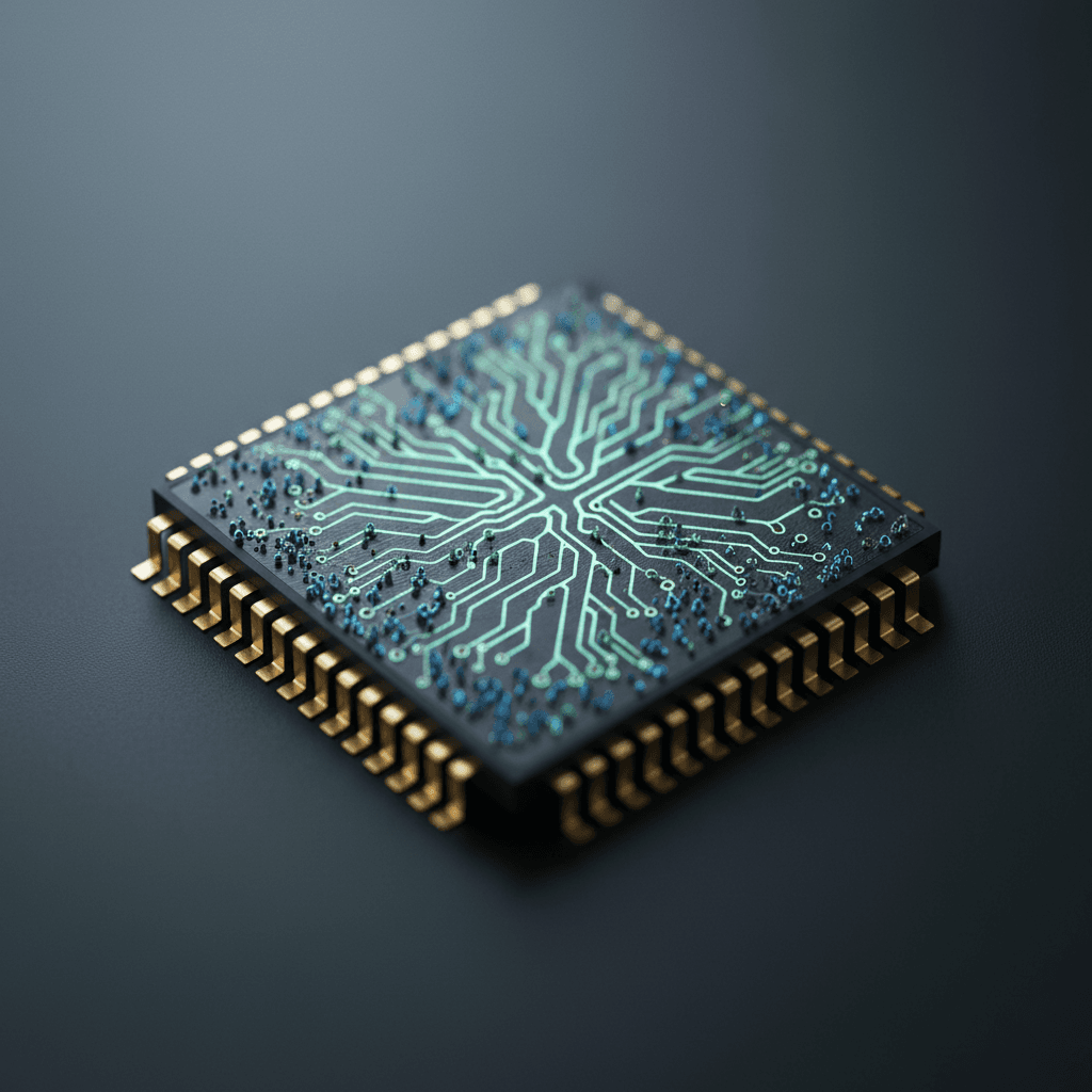
A team at the University of Cambridge has built a new kind of memristor, a tiny electronic device that imitates how neurons connect in the human brain, and it operates on switching currents roughly a million times lower than conventional oxide-based devices. The work, published this month in Science Advances, lays out a path toward neuromorphic hardware that could cut AI energy consumption by up to 70%.
That number matters right now. Hyperscalers are collectively spending north of $600 billion on data centers this year, and the bottleneck is increasingly watts, not chips. A device that slashes the power budget for AI inference at the hardware level is not an incremental improvement. It is a different category of solution.
What the Cambridge team actually built
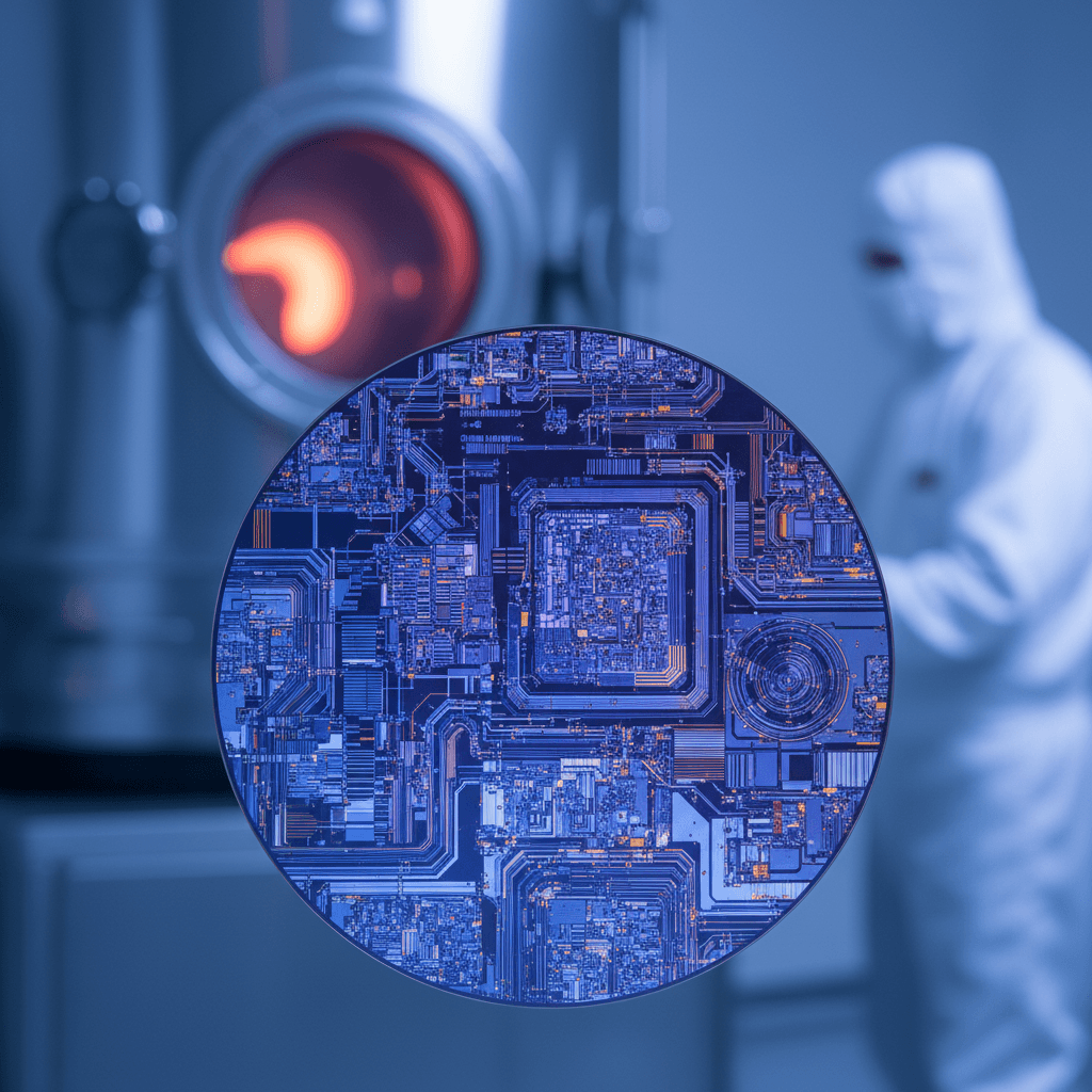
Lead researcher Dr. Babak Bakhit, from Cambridge's Department of Materials Science and Metallurgy, spent three years iterating on hafnium oxide (HfO2) thin films before hitting on the right approach. Most existing memristors work by growing and breaking tiny conductive filaments inside a metal oxide. The problem: those filaments behave unpredictably. They require high voltages, they vary from cycle to cycle, and they make large-scale manufacturing a headache.
Bakhit's team took a different route. By doping hafnium oxide with strontium and titanium, then growing the film in a two-step deposition process (adding oxygen only after the first layer was laid down), they created p-n junctions, small electronic gates, at the interface between layers. Instead of forming and rupturing filaments, the device changes resistance by shifting the height of an energy barrier at that interface.
"Filamentary devices suffer from random behaviour," Bakhit said. "But because our devices switch at the interface, they show outstanding uniformity from cycle to cycle and from device to device."
The result: switching currents about a million times lower than conventional devices. The memristors also produced hundreds of distinct, stable conductance levels and endured tens of thousands of switching cycles. They even reproduced spike-timing dependent plasticity, the biological mechanism by which neurons strengthen or weaken connections based on signal timing. That is the kind of behavior you need for hardware that genuinely learns, not hardware that simply stores and retrieves bits.
Why this matters for AI's energy problem
Conventional AI chips shuttle data back and forth between separate memory and processing units. That constant bus traffic is where most of the energy goes. Neuromorphic computing eliminates the commute by storing and processing information in the same physical location, the same way biological brains do.
The potential energy savings, up to 70% according to the Cambridge team, would be significant at data center scale. Consider that a single large language model training run can consume as much electricity as a small town uses in a year. Multiply that across the thousands of inference workloads running 24/7, and the math gets ugly fast. A hardware-level efficiency gain of this magnitude, if it scales, changes the economics of deploying AI.
Dr. Matt Wells, Senior Commercialisation Associate at Cambridge Enterprise (the university's innovation arm), put it plainly: "This new chip material has the potential to lower energy consumption of AI hardware by up to 70%. Dr. Bakhit's work is a great step towards lowering the industry's carbon footprint whilst still enabling all that AI has to bring."
Cambridge Enterprise has filed a patent on the technology.
What we don't know yet
- The fabrication temperature is too high for production. The current process requires around 700 degrees Celsius, well above standard semiconductor manufacturing tolerances. Bakhit's team is actively working on bringing this down, but until they do, the technology cannot be integrated into existing chip fabrication lines. This is a hard engineering constraint, not a minor detail.
- Retention time is limited. Lab tests showed the devices store their programmed states for about a day. For persistent memory applications, that window needs to extend considerably. For inference workloads where weights are reloaded frequently, a day might be adequate, but the paper does not address this tradeoff in detail.
- There is no system-level demonstration yet. The results are device-level measurements in a lab. Going from individual memristors to a functioning neuromorphic chip with millions of them working in concert is a separate, enormous engineering challenge.
What comes next
Bakhit said the immediate priority is solving the temperature problem. "If we can reduce the temperature and put these devices onto a chip, it would be a major step forward," he said.
The broader context here is that neuromorphic computing is one of several approaches competing to solve AI's energy crisis. Intel's Loihi chips, IBM's NorthPole architecture, and several startups are all chasing variations on brain-inspired hardware. What distinguishes the Cambridge work is the material innovation itself: a hafnium oxide formulation that is already widely used in semiconductor manufacturing (it is a standard gate dielectric in modern transistors), which could simplify the eventual integration path.
If the fabrication temperature comes down and the retention window stretches, this is the kind of material advance that does not just improve existing chips. It enables a fundamentally different architecture, one where the hardware itself learns. The chip industry is already collapsing old boundaries between design and manufacturing. Neuromorphic materials could collapse the boundary between memory and compute.
That is not hype. That is what the data says is possible. Whether it gets there depends on engineering problems that are hard but well-defined, and that is exactly the kind of problem that tends to get solved.
Juno Okafor covers quantum computing and materials science for The Daily Vibe.